(TDLR: I explore multiple ways of using flex PCBs to fix design mishaps.)
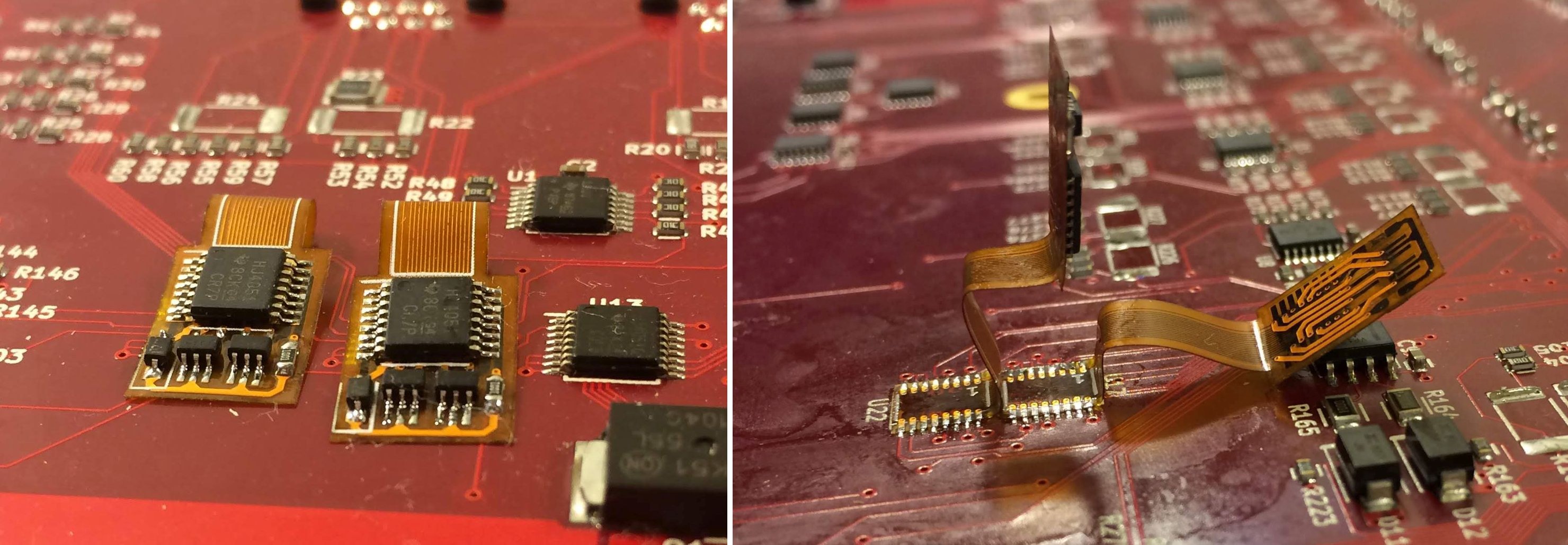
Recently I designed a circuit board that had a systematic error – a single conceptual mistake that was replicated in multiple places. These botched PCBAs were very expensive, one time builds. There was not a simple fix and I struggled to find a way to modify the PCBA that was both robust and professional in appearance. Dozens of long bodge wires and glued on components do not fit this description. Bodge wiring would also have required hours of tedious soldering. This job needed a different solution. I had considered creating a small PCB that could be soldered in place of one or more of the IC’s on the board; but this approach had several drawbacks:
1. In many places there wasn’t space for the extra circuitry.
2. The spaces that were available were of a varying shape.
3. The pitch of the pins was too small for castellations (0.65mm).
Recently, “cheap” flexible PCBs have become available from China. I realized that this was the solution to my problem. A single flex circuit design could be “bent” to fit every location.
In this post I will not just document the one technique that I used to solve my specific problem; but, I will also explore this technique more generally.
Attaching The Bodge PCB
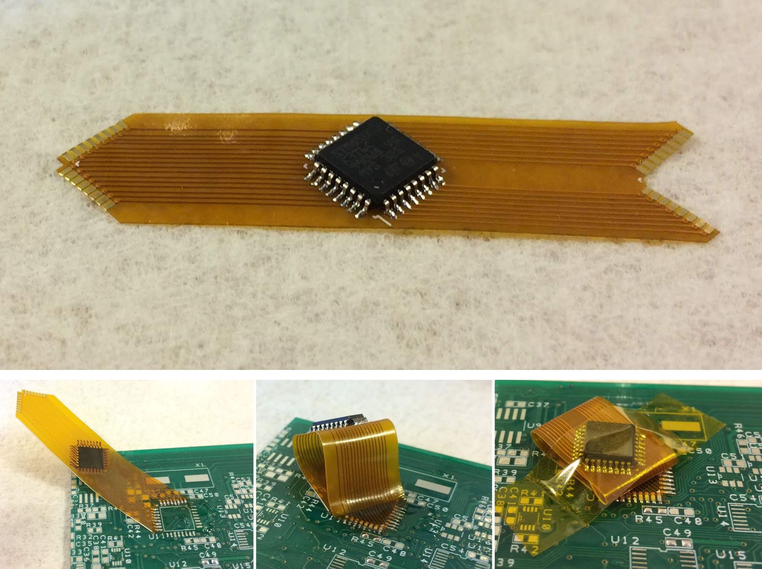
I needed to add circuitry around several ICs. But, each IC location had different clearance around it. The flex PCB allowed me to have a board level footprint no larger than the original IC. The added circuitry could float above the board and be secured to the board as necessary. Obviously, I needed pads on the flex PCB that matched the footprint on the original PCB – but, how should I solder the two PCBs together? I could only think of two methods – exposed pad and blind pad, both of which I describe below.
A. Exposed Pad (Cut the flex to expose the edge of the pads.)
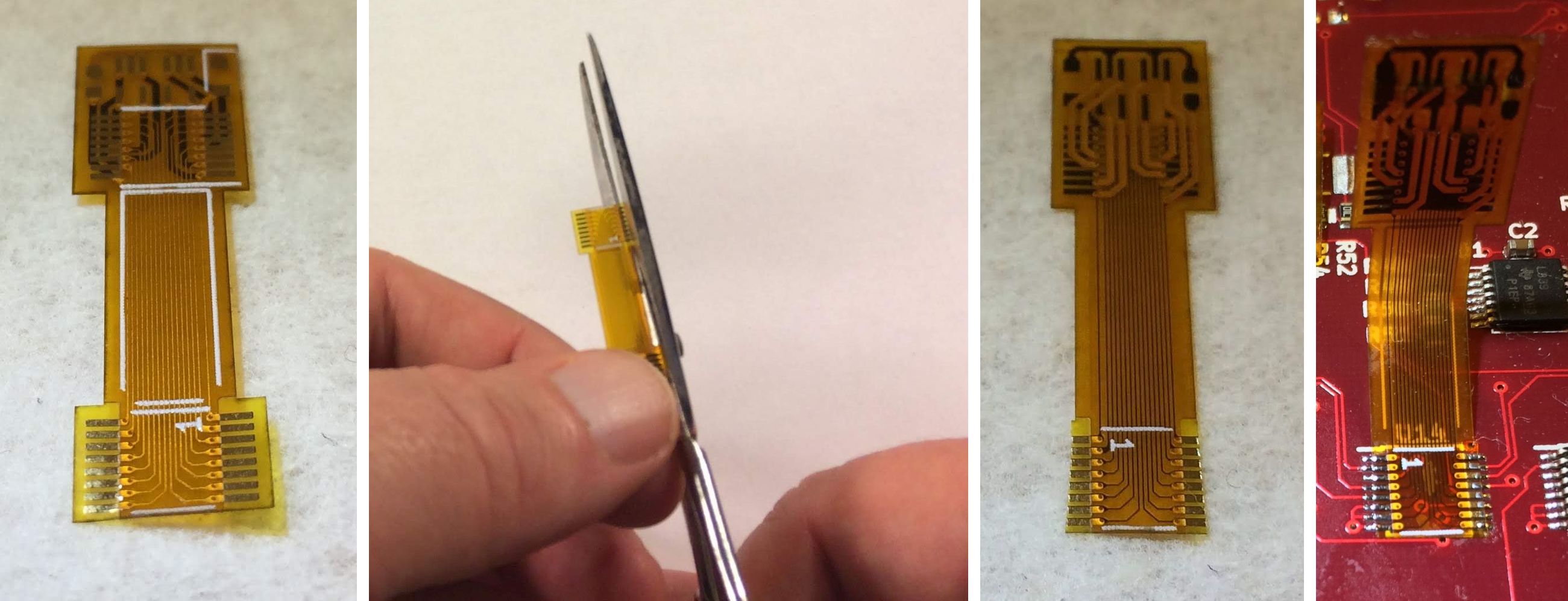
Exposed Pads
I felt that if the pads were brought to the edge of the flex PCB soldering would be much easier, in the same way that it is easier to solder an SOIC than a BGA. I did not really consider trying to make castellations. My thinking was that if I put pads on both sides of the flex PCB, the solder would easily bridge to the top side pad. However, I had difficulty bridging the solder to the top pad. But it wasn’t necessary; the solder quite easily flowed onto the bottom side pad.
Perhaps it was a communication problem, but, the board house seemed either unwilling or unable to cut the board outline through the pads. To bring the pads to the edge of the PCB, I cut the flex PCB with scissors. Soldering the cut flex PCB was trivially easy, without any “tricks” required.
B. Blind Pad (Solder the PCBs without cutting the flex.)
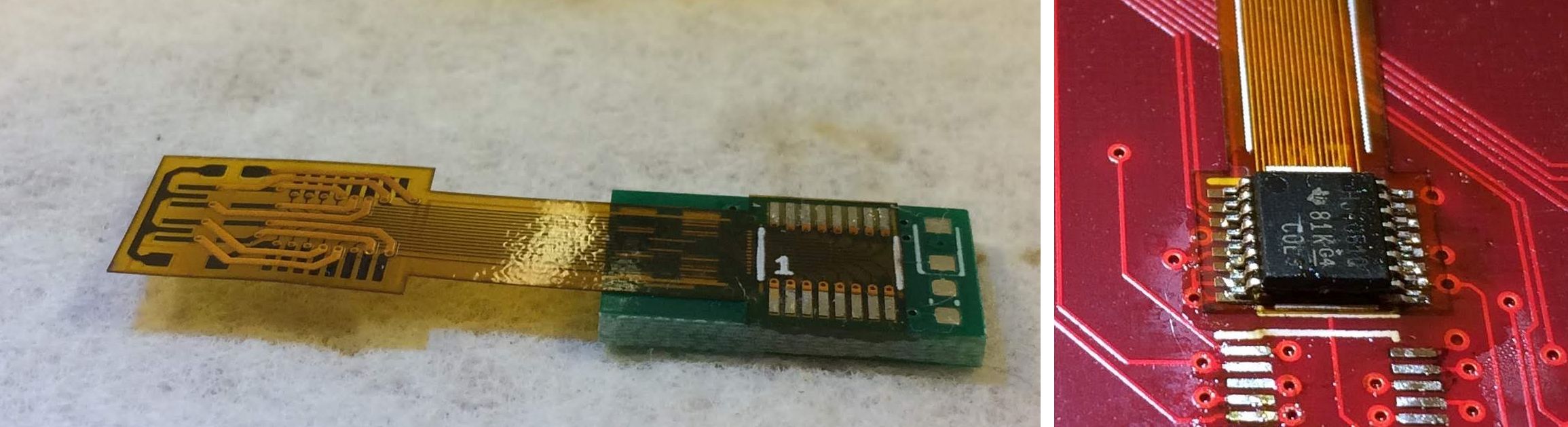
Blind Soldering The Pads
What if the pads are not at the edge of the flex PCB? I was less confident that this would work because the pads were not accessible for soldering or inspection. But, I was able to work out a technique that seemed to work reliably. Continuity testing showed 24 out of 24 solder joints that I made were good and without shorts.
To solder blind pads,
1. Start by tinning the pads of both the flex and hard PCB.
2. Remove all of the excess solder from the pads of both PCBs with solder wick/braid.
3. Align the flex pads with the pads on the hard PCB.
4. Use a soldering iron with a chisel tip. From the top side, press each flex PCB pad down onto the corresponding hard PCB pad, one at a time. Hold the iron down firmly for a moment, but then lift it quickly. When I did this, the flex pads seemed to stay depressed after I lifted the iron. I assumed that this indicated a good solder connection.
I found out the hard way that excess solder on the pads will “squish” out and bridge across pads. Excess solder also made it difficult to keep the pads aligned before soldering. Note: You might want to use a non-heated implement to hold the flex down as you lift the iron. But, I did not do this and it seemed to work well enough.
Bridges
On a couple of solder joints I created a solder bridge between pins. Conveniently, I was able to see these bridges through the transparent flex PCB. To clear the short, I used a hot chisel tip soldering iron to “squeegee” the solder bridge out from under the flex. I placed the tip of the iron on top of the flex, inboard of the bridge, and slowly dragged the iron tip to the edge of the flex. After several tries I was able to clear the bridge. This proved that I could melt the solder through the flex PCB – i.e. melt the solder under the flex by placing an iron on top of the flex.
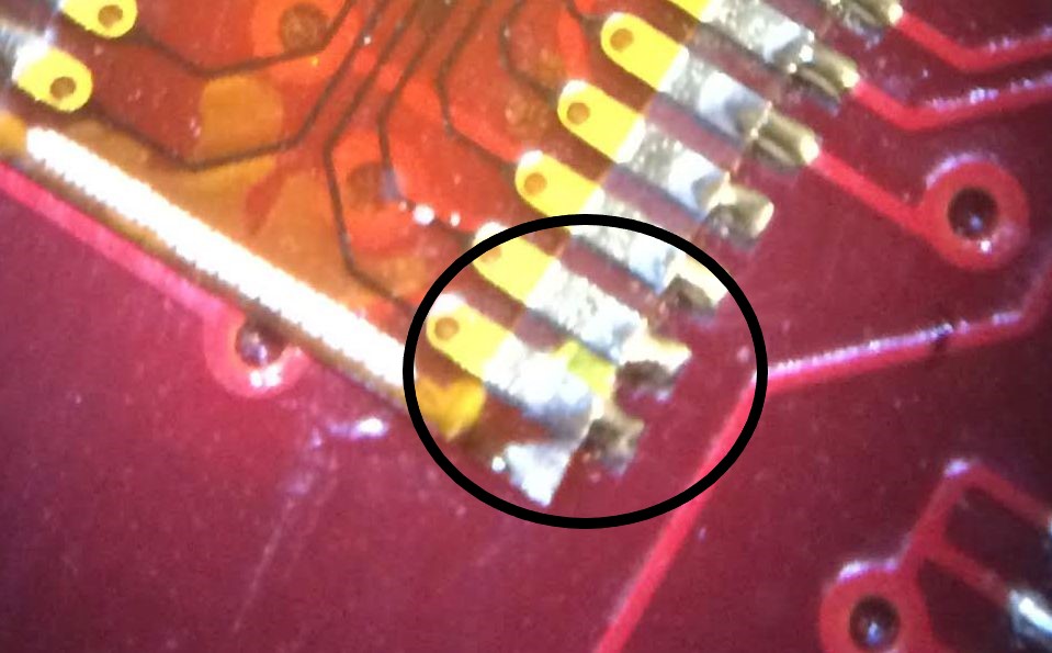
Solder Bridge Visible Through Flex PCB
What About Quad-Sided Footprints?
The footprint that I needed to bodge was a TSSOP, but what about a QFP? With pads in two parallel rows (TSSOP), it was obvious how to cut the pads so that they came to the edge of the flex PCB. With a quad-sided part it was not so obvious. A simplistic approach made the circuitry overhang the pads making it difficult to solder. With some mental origami, I came up with a configuration that avoided this difficulty. The trick was to flip to rows of the pads to the bottom side of the flex PCB. In this way I could solder all of the pads without obstruction.
The Easier Way
The Hard Way (Mocked Up)
Purchasing The Flex PCBs
I looked at OSHPARK but their “per square inch” pricing wasn’t practical for me – I needed dozens of flex PCBs. In the end I went with PcbWay, they have a minimum of about $120 but I was able to get over a hundred small flex PCB’s for this price.
Money Saving Tip:
You can combine multiple flex PCB designs into one and then simply use scissors to cut them apart.
Conclusion
This bodge procedure worked fantastically and only cost about $125. Using a custom flex PCB has only recently become practical. I wish I had this option years ago when I misnumbered the pins on a large quad footprint – many copper spiders were created that week!